Introduction
You have finished your schematic, routed the layout, and exported the Gerber files — now what? For most electronics engineers and product startups in India, the gap between a finished design and a working prototype board is where projects slow down. This guide walks you through the complete PCB prototyping process: preparing your files, choosing quantities and specifications, what happens inside the fab, and how to avoid the mistakes that cause costly re-spins. Whether you are building an IoT device, an LED driver, or an industrial controller, getting the first prototype right saves weeks of iteration.
Step 1: Prepare Clean Gerber Files
Your fabrication house can only build what your files describe. Before sending anything, export the full Gerber package (RS-274X format) along with the NC drill file, and run it through a Gerber viewer to check what the manufacturer will actually see. The most common file problems we see at OM Electronics are missing drill files, outdated board outlines, and solder mask layers that do not match the copper. Include a fab notes file that states layer count, board thickness (1.6 mm is standard), copper weight (1 oz is typical), surface finish (HASL or ENIG), and solder mask colour.
Step 2: Choose the Right Prototype Quantity and Specs
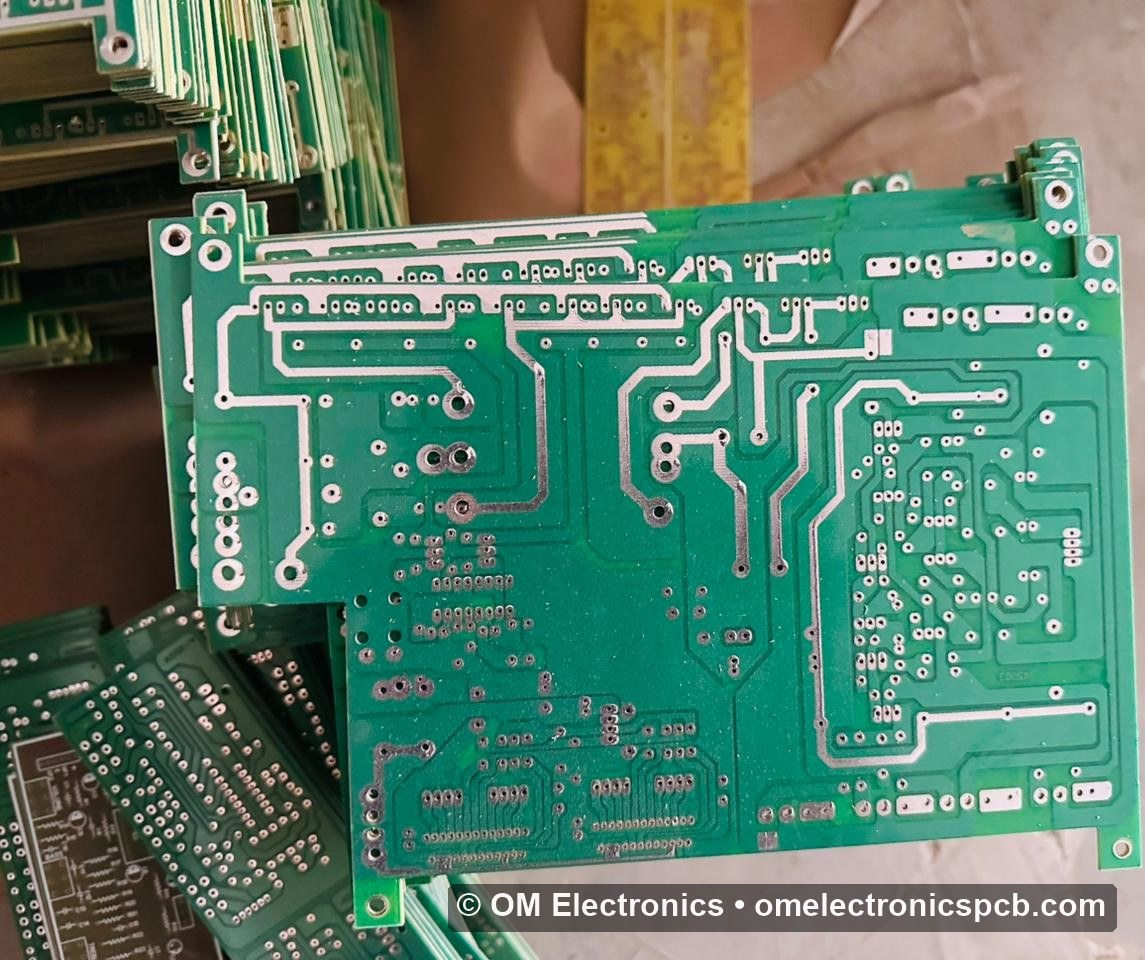
For a first prototype run, 5 to 10 pieces is the sweet spot — enough boards to assemble a few units, keep one bare board for reference, and survive an assembly mistake. Resist the temptation to over-specify: a 2-layer FR4 board with standard 6/6 mil trace/space and HASL finish is faster and cheaper to fabricate than an aggressive design, and it is enough for most prototypes. Move to 4 layers only when you genuinely need a ground plane for signal integrity or power distribution. If your design has fine-pitch BGAs or impedance-controlled traces, mention it upfront so the fab can flag capability issues before production starts.
Step 3: What Happens at the Fab — and How Long It Takes
Once your files pass DFM (Design for Manufacturability) review, the board goes through imaging, etching, drilling, plating, solder mask, silkscreen, surface finish, and electrical testing. A quick-turn prototype run at a local PCB manufacturer in Mohali or Derabassi typically ships in 3–5 working days, compared to 2–3 weeks when importing from overseas — and you skip customs delays and freight costs entirely. Working with a nearby manufacturer also means you can discuss DFM feedback directly with an engineer instead of a ticketing system, which matters most at the prototype stage when changes are frequent.
Step 4: Common Prototyping Mistakes to Avoid
Most prototype failures are not fabrication defects — they are design and communication issues that a little discipline prevents. Watch out for these:
- Skipping the DFM check. If your fab offers a free design review, use it. Ten minutes of engineer feedback catches acid traps, sliver traces, and annular ring violations before they become scrap.
- Wrong footprints. Print your layout 1:1 on paper and place real components on it. A mirrored connector or wrong-pitch IC footprint is the most common reason a first prototype never powers up.
- No test points. Add accessible test points for power rails, ground, and key signals. Debugging a dense board without them wastes hours.
- Ignoring panelization. If you plan to assemble by machine later, discuss panel size, fiducials, and tooling holes at the prototype stage so production needs no redesign.
- Ordering exactly the number you need. Boards get damaged during rework and bring-up. The extra two or three boards cost little; a re-order costs a week.
Step 5: From Prototype to Production
Once your prototype works, resist the urge to jump straight to a large order. Run a small pilot batch of 50–100 boards first — it validates the fab’s process at volume, surfaces assembly and yield issues, and gives you real units for field testing and certification. Lock your BOM with approved alternates for hard-to-source parts, freeze the Gerber revision, and document every change between the prototype and pilot revisions. A good manufacturer will keep your tooling and stack-up on file, so repeat production orders in India can ship in days rather than weeks. This is also the right time to negotiate volume pricing: fabricating and assembling locally means shorter feedback loops, no customs risk, and quick reruns when demand spikes.
How to Choose a Prototyping Partner
Not every fab is set up for prototypes. Production-focused factories often quote long lead times and high tooling charges on small quantities. When evaluating a prototyping partner, ask four questions: What is the genuine quick-turn lead time for a 2-layer and a 4-layer board? Is engineering support available to discuss DFM issues directly? Are tooling and setup charges waived or reduced for repeat orders? And can the same facility scale to your production volumes so you are not re-qualifying a new vendor after the prototype succeeds? With over 25 years of PCB fabrication experience, OM Electronics answers yes to all four — from single-piece prototypes to bulk production of single layer, double layer, aluminium, and metal-core PCBs.
Frequently Asked Questions
How much does PCB prototyping cost in India? A small 2-layer prototype run (5–10 boards, up to 100 mm × 100 mm) usually costs a few hundred to a couple of thousand rupees depending on size, finish, and turnaround. Local fabrication avoids import duties and shipping, which often halves the landed cost versus overseas prototypes.
What files does a PCB manufacturer need? Gerber files (all copper, mask, silkscreen, and outline layers), the NC drill file, and a short fab note listing material, thickness, copper weight, and finish. For assembly, add the BOM and pick-and-place file.
How fast can I get a prototype PCB near Chandigarh? OM Electronics serves Mohali, Zirakpur, Derabassi, Chandigarh, and Panchkula with quick-turn prototype fabrication — standard 2-layer prototypes are typically ready in 3–5 working days.
Can I get PCB assembly along with prototype fabrication? Yes. Supplying your BOM and pick-and-place file with the Gerbers lets the fab quote bare boards and assembled prototypes together, which is faster and usually cheaper than assembling separately.
Do aluminium and metal-core PCBs need a different prototyping process? The file requirements are the same, but thermal substrates have different drilling and V-scoring parameters — tell the fab it is an MCPCB upfront. OM Electronics prototypes FR4, aluminium, and metal-core boards in the same facility.
Key Takeaways
- Verify your Gerber and drill files in a viewer before submitting — file errors are the number one cause of prototype delays.
- Order 5–10 boards with standard specs (2-layer, 1.6 mm FR4, HASL) unless your design truly needs more.
- A local Indian fab turns prototypes around in 3–5 days and gives you direct engineer-to-engineer DFM feedback.
- State special requirements — impedance control, fine-pitch parts, ENIG — upfront so they are caught in DFM review, not on the line.
Conclusion
Prototyping is where good designs become real products, and the fastest path runs through clean files, sensible specifications, and a manufacturer you can actually talk to. OM Electronics offers quick-turn PCB prototyping and full production runs from our facility near Chandigarh, serving customers across Mohali, Zirakpur, Derabassi, and all of India. Upload your Gerber files at omelectronicspcb.com or contact our team for a free DFM review and same-day quote on your next prototype.
For more PCB guides, read us on our Blogspot blog and Medium, or follow OM Electronics on X (Twitter) for manufacturing updates and offers.